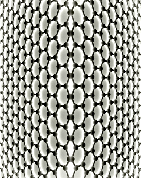
Big step in printed graphene
 Researchers have printed electronic transistors using layered materials, opening up a new way to create next-gen devices.
An international team based in Dublin has used standard printing techniques to combine graphene flakes as electrodes with other layered materials, tungsten diselenide and boron nitride as the channel and separator (two important parts of a transistor) to form an all-printed, all-layered materials, working transistor.
The flakes are a few nanometres thick but hundreds of nanometres wide. The layering of various materials creates electronic properties like conducting (in the case of graphene), insulating (boron nitride) or semiconducting (tungsten diselenide), as the building blocks of electronics.
While the performance of these printed layered devices cannot yet compare with advanced transistors, the team believe there is a wide scope to improve the performance of their printed TFTs beyond the current best.
“In the future, printed devices will be incorporated into even the most mundane objects such as labels, posters and packaging,” says researcher Professor Jonathon Coleman.
“Printed electronic circuitry will allow consumer products to gather, process, display and transmit information: for example, milk cartons will send messages to your phone warning that the milk is about to go out of date.”
All of the layered materials were printed from inks created using a liquid exfoliation method previously developed by Professor Coleman and already licensed.
Using liquid processing techniques to create the layered materials inks is especially advantageous in that it yields large quantities of high quality layered materials which helps to enable the potential to print circuitry at low cost.


 Print
Print